
Technical Capabilities
Manufacturing Excellence
in Every Specification
From 2-layer prototypes to 32-layer HDI production — explore our full range of PCB and PCBA manufacturing capabilities.
Technical Capabilities
From 2-layer prototypes to 32-layer HDI production — explore our full range of PCB and PCBA manufacturing capabilities.
| Parameter | Capability | Standard |
|---|---|---|
| Layer Count | 2 – 32 layers | Advanced |
| HDI | Any-layer, 1+N+1, 2+N+2 | Advanced |
| Min Trace / Space | 3 / 3 mil (0.075 / 0.075 mm) | Fine-line |
| Min Mechanical Drill | 0.15 mm | Standard |
| Min Laser Drill | 0.075 mm | Microvia |
| Impedance Control | ±5% (TDR tested) | Precision |
| Board Thickness | 0.2 mm – 6.0 mm | Full Range |
| Max Board Size | 600 mm × 800 mm | Large Format |
| Aspect Ratio | 12:1 | Standard |
| Copper Weight | 0.5 oz – 12 oz | Heavy Copper |
| Finish Type | IPC Standard | Best For |
|---|---|---|
| ENIG (Electroless Nickel Immersion Gold) | IPC-4552 | Fine-pitch, wire bonding, long shelf life |
| OSP (Organic Solderability Preservative) | IPC-4554 | Cost-effective, RoHS compliant |
| HASL Lead-Free | IPC-4553 | General purpose, excellent solderability |
| Immersion Silver | IPC-4556 | High-frequency RF, fine-line |
| Immersion Tin | IPC-4555 | Press-fit connectors, flat surface |
| Hard Gold (Electrolytic) | IPC-4552 | Edge connectors, high-wear contacts |
| Material | Tg (°C) | Td (°C) | Applications |
|---|---|---|---|
| Standard FR-4 | 135 – 140 | 310 | Consumer electronics, general purpose |
| High-Tg FR-4 | 170 – 180 | 350 | Automotive, industrial, lead-free soldering |
| Rogers 4350B / 4003C | 280 | 390 | RF, microwave, high-frequency |
| Aluminum (Metal Core) | 130 – 150 | — | LED lighting, power electronics |
| Ceramic (Al₂O₃ / AlN) | — | — | High-power, high-thermal applications |
| Polyimide | 250 | 420 | Flexible circuits, high-temp applications |
Multiple lamination cycles for complex HDI stackups with blind and buried via structures.
Stub removal for high-speed signals. Controlled depth drilling with ±0.05mm accuracy.
Via filling with conductive or non-conductive epoxy, plated over for BGA pad placement.
Combined rigid and flexible sections in one board. Polyimide flex with FR-4 rigid areas.
Plated board edges for shielding, grounding, and mechanical protection.
Precision mechanical machining for mounting holes with tight depth tolerance.
| Parameter | Capability |
|---|---|
| SMT Lines | 8 fully automated high-speed lines |
| Placement Capacity | 8,000,000 placements per day |
| Component Range | 0201 (0.6×0.3mm) to 55×55mm BGA/QFP |
| Minimum Pitch | 0.3mm (QFP/QFN), 0.25mm (BGA) |
| Assembly Types | SMT, THT, Mixed, Flex, Rigid-Flex |
| Solder Paste Inspection | 3D SPI on all lines |
| AOI Inspection | 3D AOI — 100% of boards |
| BGA Inspection | X-Ray (2D + CT tomography available) |
| In-Circuit Test | ICT — flying probe and bed-of-nails |
| Functional Test | FCT — custom test fixtures built in-house |
| Conformal Coating | Selective spray and manual brush |
| Potting / Encapsulation | Epoxy and silicone potting available |
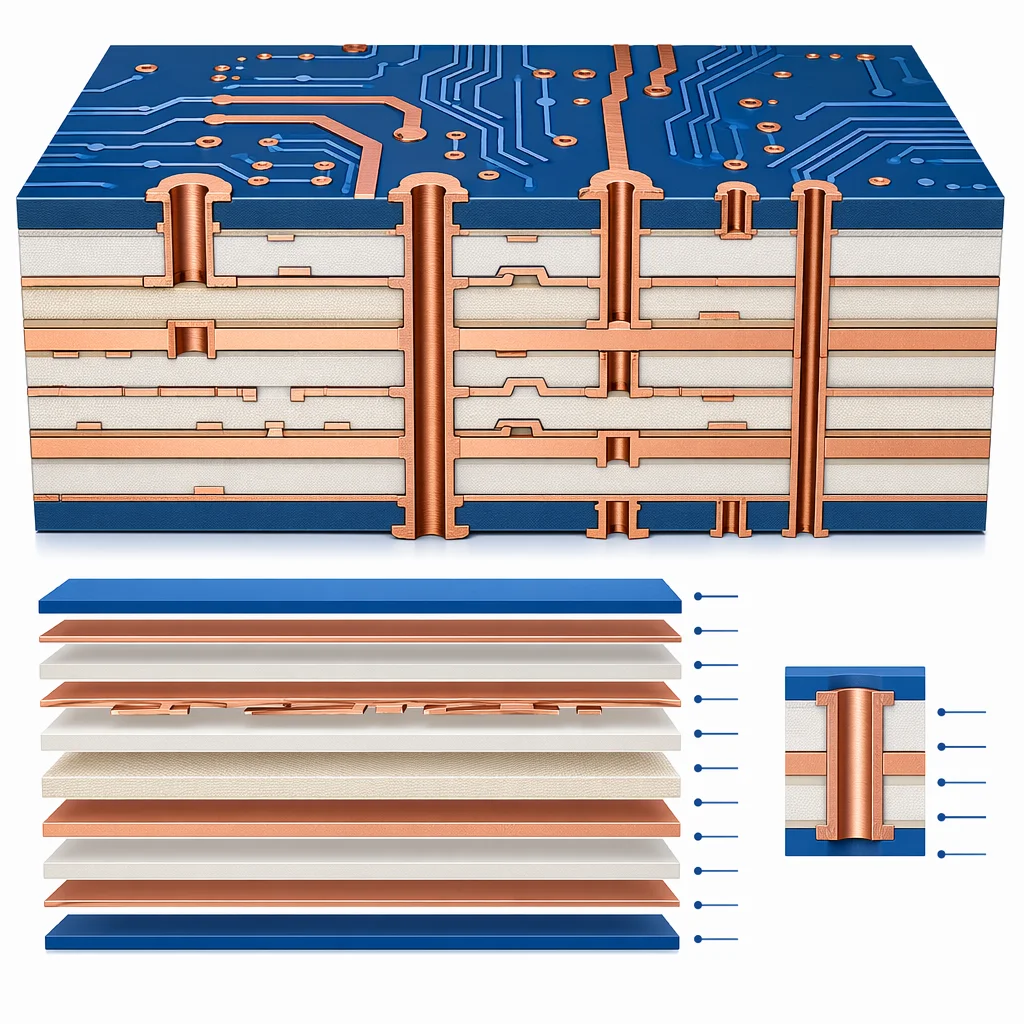
Technology
Every layer precisely aligned and bonded. Our advanced lamination process ensures perfect registration and impedance control across all 2 to 32 layers. Each via type — through-hole, blind, buried, or microvia — is optimized for your specific design requirements.
Request PCB QuoteProcess
From solder paste printing to final inspection — each step monitored and controlled. 3D SPI checks every paste deposit. High-speed placement with 8-head gantry machines. 10-zone reflow ovens with nitrogen atmosphere for perfect soldering.
Request PCBA Quote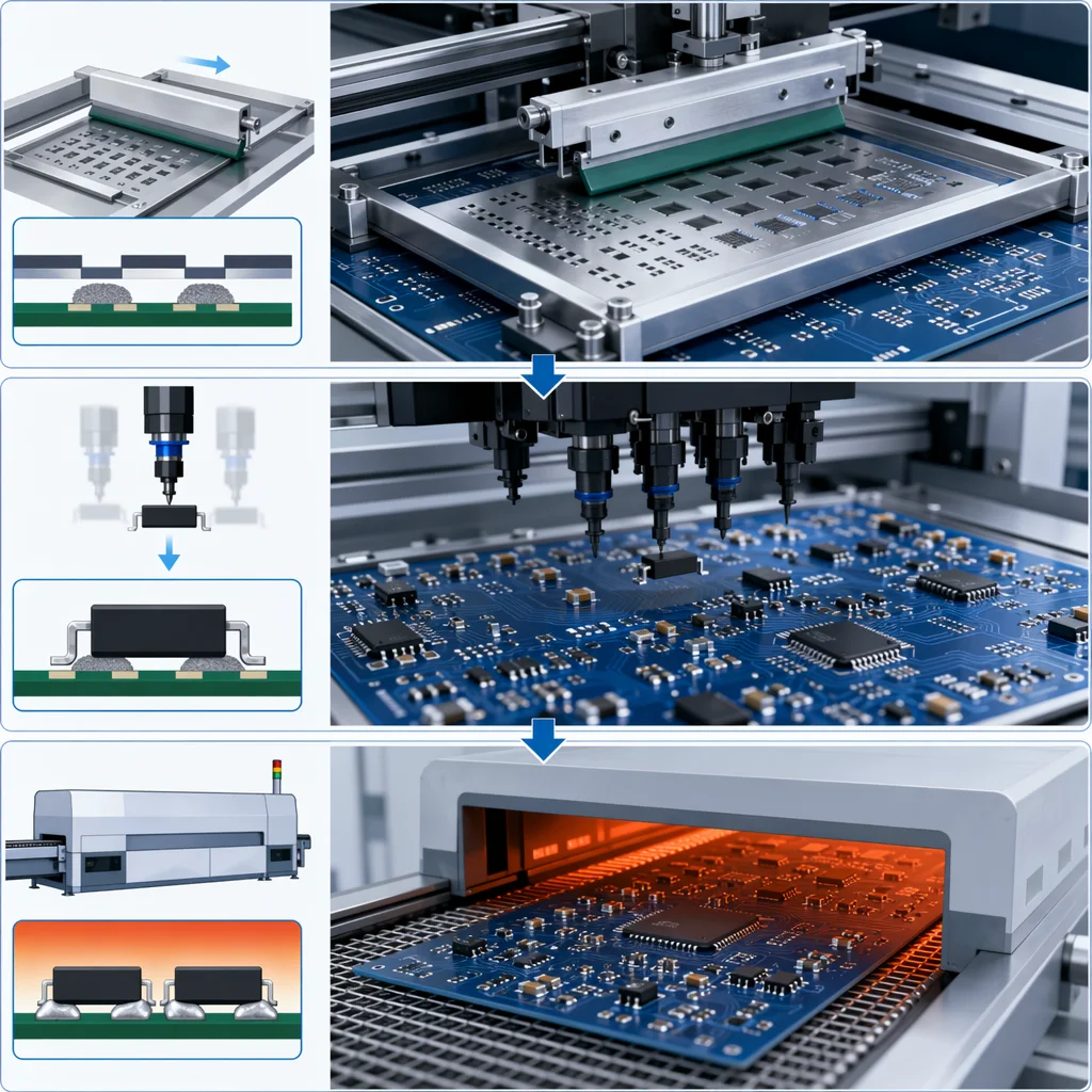
Value-Added
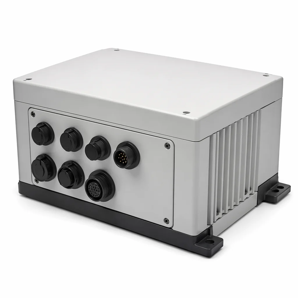
Beyond PCBs and PCBA — we assemble your complete product. Enclosure integration, wiring harnesses, functional testing, labeling, and customized packaging. Your product ships ready for your customer.
Send us your specs — Gerber files, BOM, assembly drawings. Our engineers will review and respond within 24 hours.
Submit Your Specs
Tell us about your project. We'll respond within 24 hours.